AMD RDNA 3 ARCHITECTURAL DEEP DIVE
Taking a dip in the pool with the upcoming RX 7900-series
Get ready for our third and final round of graphics architectural deep dives. Two months ago, we spilled the beans on Nvidia’s Ada Lovelace architecture. Last month, we did the same for Intel’s Arc Alchemist. Last to the party, but perhaps the most interesting in its approach in the realm of GPU design is AMD’s RDNA 3, premiering with the Radeon RX 7900 XTX and Radeon 7900 XT.
Thanks to its use of chiplets, the RDNA 3 architecture fundamentally changes several of the key design elements. AMD pioneered chiplets in the consumer realm with its Zen 2 (Ryzen 3000) CPUs. That has enabled AMD to deliver more cores and better performance, giving Intel some much-needed competition. Now it’s looking to do the same with GPUs and graphics cards.
It’s not an easy transition to make and, of course, GPUs are fundamentally quite different from CPUs. Whereas CPUs typically come with a few dozen general-purpose cores at most—up to 96 with the latest AMD Genoa EPYC processors—GPUs already have thousands of specialized shader ‘cores’, each of which needs access to the large data sets involved with graphics work, such as the textures and the geometry.
So, it’s time to don your swimsuit as we dive into the latest RDNA 3 architecture to see what makes it tick.
–JARRED WALTON
THE GPU CHIPLET ERA BEGINS
For now, AMD has only revealed one specific design for RDNA 3, the Navi 31 GPU. It consists of two separate pieces of silicon, the Graphics Compute Die (GCD) and the Memory Cache Die (MCD). The names already provide a good indication of how AMD chose to split up the normal monolithic chunk of silicon that makes up a GPU into multiple chiplets.
The GCD houses the Compute Units (CUs) that provide the raw number crunching capabilities of AMD’s GPUs. It also houses other core functionality like video codec hardware, display interfaces, texturing units, render outputs, and the PCIe connection. So far that’s no different than previous GPUs, but with RDNA 2 as an example, the GPU also housed a large chunk of L3 cache—the Infinity Cache—along with memory controllers that link to external GDDR6 memory.
With RDNA 3, or at least Navi 31 (see the side panel on Future RDNA 3 GPUs), the GCD has up to 96 CUs, which is where the typical graphics processing occurs. It also has the Infinity Fabric along the top and bottom edges of the chip that provide an extremely wide and fast link to all the MCDs. It can link with up to six MCDs and, in that configuration, the total Infinity Fabric bandwidth is a staggering 5.3 TB/s.
Meanwhile, the MCDs do exactly what their name implies: Each houses a large 16MB chunk of L3 cache, along with the physical GDDR6 memory interface. They also contain Infinity Fabric links to connect to the GCD, which you can see in the die shot along the center-facing edges of the MCDs.
What’s the point in splitting up the functionality between the GCD and MCDs? We’re glad you asked, as it’s the key point of a chiplet approach. The GCD will use TSMC’s 5nm N5 node, basically, the latest and greatest full production node that’s currently available—4N, N4P, and N4 are all derived from N5.
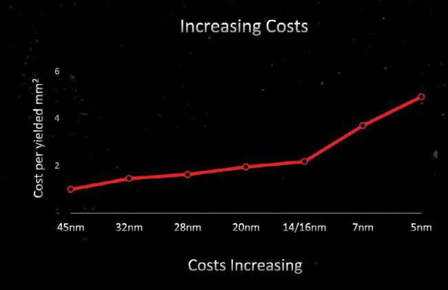
The motivation behind AMD’s chiplet strategy is all about improving yields and flexibility while reducing costs.
The MCDs, on the other hand, use TSMC’s N6, a derivative of the previous 7nm N7 process node.
There are several important reasons for the split. First and foremost, N6 is a lot cheaper than N5. TSMC doesn’t publicly disclose contract pricing, but there are indications that 5nmclass wafers cost about twice as much as 7nm-class wafers. Second, the scaling of certain elements has slowed down or almost entirely halted with smaller process nodes. External interfaces like those for GDDR6 would be just as large on N5 as on N6. The scaling of cache cells has also slowed down, so 16MB of L3 cache on N5 would be nearly as large as 16MB on N7.
Beyond cost and scaling, there’s another benefit to the split: chip yields. Creating a larger chip means there’s a much higher potential for any given die to contain a defect—there are relatively consistent impurities with silicon wafers. To avoid having a single defect result in a useless die, large chips need the ability to disable portions of the die. That can result in more complex routing and other redundancies, which in turn adds to the cost.